

| Features | Capability | Description | Patterns |
| Layer count | 1-64 Layers | The number of copper layers in the PCB | |
| Controlled Impedance | 4/6/8/10/12/14/16/18/20/.../32/.../48/.../56/.../64 layers | User Guide to the UC PCB Impedance Calculator UC PCB Impedance Calculator | |
| Impedance Tolerance | ±10% | — | |
| Material | FR-4 | Grade A laminates from suppliers including Nan Ya, KB, Shengyi, etc. | 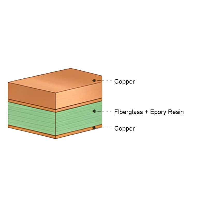 |
| Aluminum-Core | 1-layer Aluminum-core PCBs | 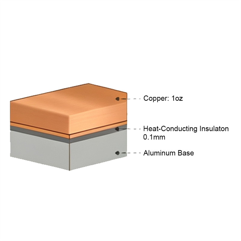 |
|
| Copper-Core | 1-layer copper-core PCBs with direct heatsink contacts to core (≥ 1 × 1 mm) | 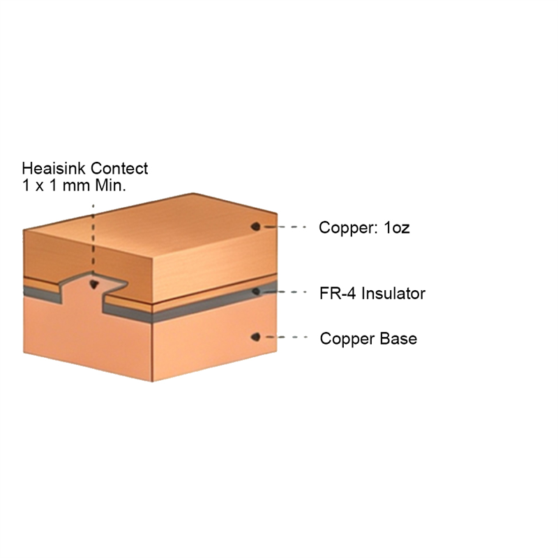 |
|
| RF PCB | 1 oz copper, 2-layer RF PCBs with Rogers and PTFE cores | 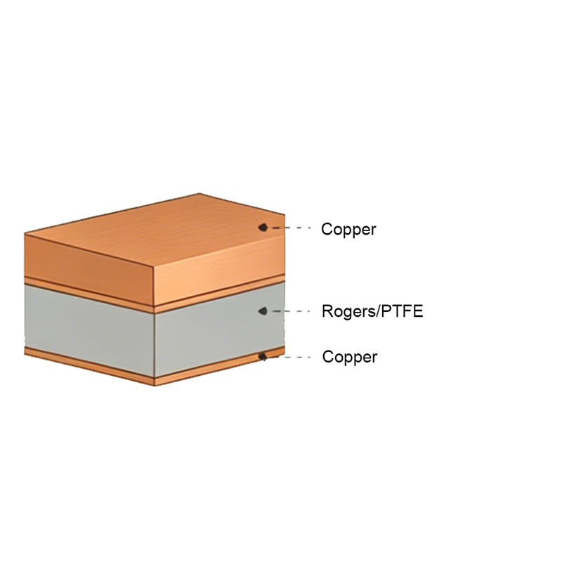 |
|
| FR-4 Dielectric Constants | 4.5 (2-Layer PCB) | 7628 Prepreg 4.43313 Prepreg 4.12116 Prepreg 4.16 | |
| Maximum Dimensions | FR4(1-layer): 606 × 510 mmFR4(2-layer): 670 × 600 mmFR4(4-layer): 663 × 593 mmFR4(6-layer and above): 656 × 586 mmRogers / PTFE Teflon PCB: 590 × 438 mmAluminum PCB: 602 × 506 mmCopper PCB: 480 × 286 mm | These limits apply to PCBs with thickness ≥ 0.8 mm maximum.The thinner FR4 PCBs are 599 × 497 mm maximum.2-layer FR4 PCBs can reach a maximum size of 1020 × 600 mm.4-layer FR4 PCBs can reach a maximum size of 1016 × 596 mm. | 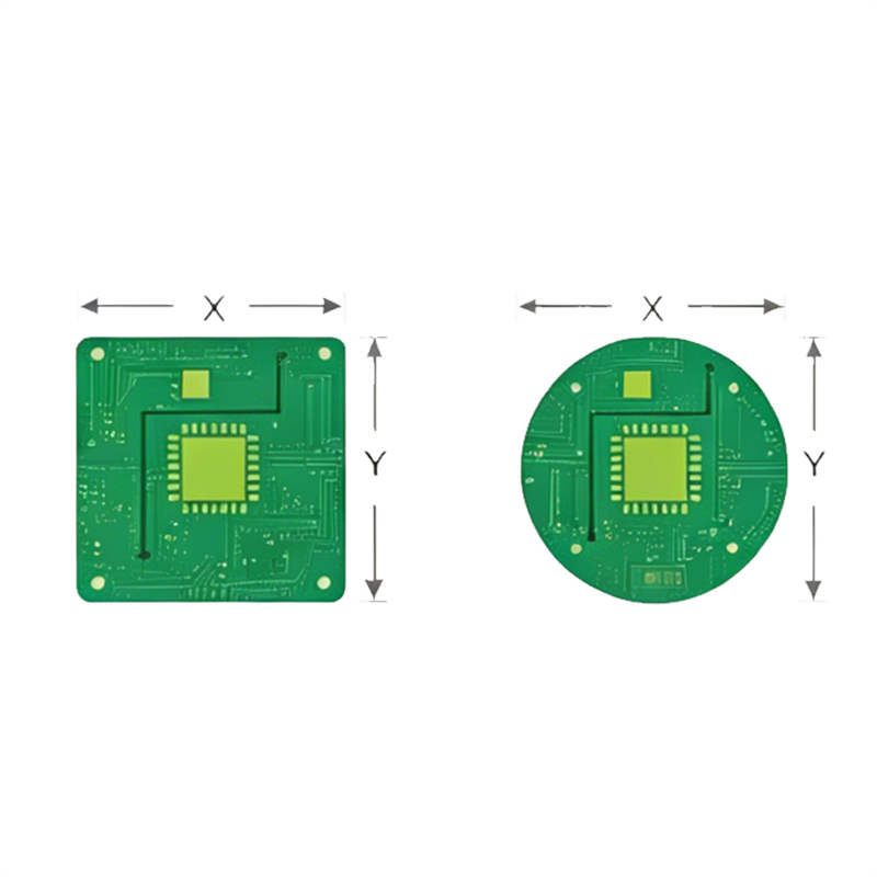 |
| Minimum Dimensions | FR4/Rogers/PTFE: 3 × 3 mmCastellated / Plated Edges: 10 × 10 mmAluminum/Copper PCB: 5 × 5 mm | These limits apply to PCBs with thickness ≥ 0.6 mm.Manual review required for thinner PCBs.Panelization is recommended for small-sized boards. | |
| Dimension Tolerance | ±0.1mm | ±0.1mm (Precision) and ±0.2mm (Regular) for CNC routing, and ±0.4mm for V-scoring | |
| Thickness | 0.4 – 4.5 mm | Thickness for FR4 are: 0.4/0.6/0.8/1.0/1.2/1.6/2.0 mm (2.5 mm and above are for 12+ layer PCBs only) | 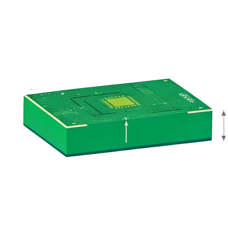 |
| Thickness Tolerance (Thickness≥1.0mm) | ± 10% | e.g. For the 1.6mm board thickness, the finished board thickness ranges from 1.44mm (T-1.6×10%) to 1.76mm (T+1.6×10%) | |
| Thickness Tolerance (Thickness<1.0mm) | ± 0.1mm | e.g. For the 0.8mm board thickness, the finished board thickness ranges from 0.7mm (T-0.1) to 0.9mm (T+0.1) | |
| Finished Outer Layer Copper | 2-layer: 1 oz / 2 oz / 2.5 oz / 3.5 oz / 4.5ozMulti-layer: 1 oz / 2 oz | — | 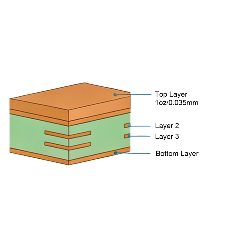 |
| Finished Inner Layer Copper | 0.5 oz / 1 oz / 2 oz | Finished copper weight of inner layer is 0.5oz by default. | 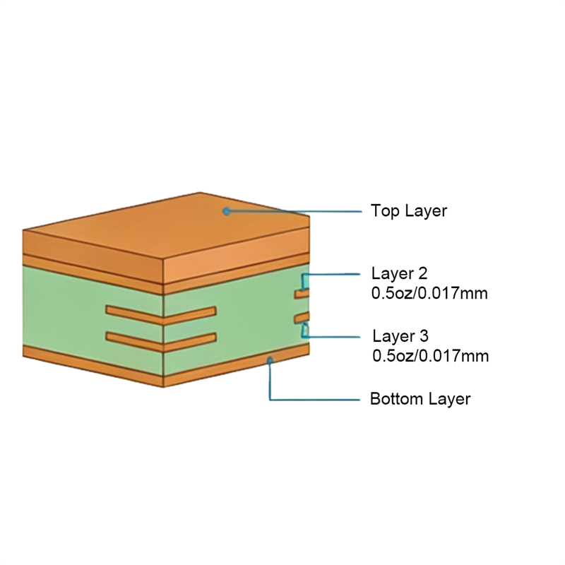 |
| Soldermask | Green, Purple, Red, Yellow, Blue, White, and Black. | We use LPI (Liquid Photo Imageable) solder mask. This is the most common type of mask used today.Heat-cured ink soldermask is usually found on low-cost, single-sided PCBs. | |
| Surface Finish | HASL (leaded / lead-free), ENIG, OSP (copper core boards only) | FR4 has all three finishes available, 6+ layers and RF boards only have ENIG.Aluminium core boards only have HASL. Copper core boards only have OSP. |
| Features | Capability | Description | Patterns |
| Drill Diameter | 1-layer: 0.3 – 6.3 mm2-layer: 0.15 – 6.3 mmMultilayer: 0.15 – 6.3 mm | Holes with diameter ≥ 6.3 mm are CNC routed from a smaller drilled hole.Min. drill diameter for 2+ or more-layer PCBs is 0.15mm (more costly).Min. drill diameter for aluminum-core PCBs is 0.65 mm.Min. drill diameter for copper-core PCBs is 1.0 mm. | 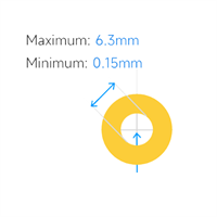 |
| Hole size Tolerance | Through-holes: +0.13 / -0.08 mmPress-fit holes: ±0.05 mm (Finished hole size: 0.55-1.025mm. Multilayer ENIG boards only. Mention the specific holes in PCB Remark) | e.g., for the 0.6mm hole size, the finished hole size between 0.52mm to 0.73mm is acceptable.To avoid soldermask or tin stuck in the hole, recommended PTH size ≥ 0.5mm. | 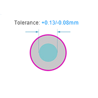 |
| Average Hole Plating Thickness | 18µm | Standard copper plating thickness inside plated holes. | |
| Hole Position Tolerance | ±0.05 mm | Deviation tolerance of hole center position. | |
| Blind/Buried Vias | Not supported | Currently we don't support Blind/Buried Vias, only make through holes. | 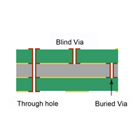 |
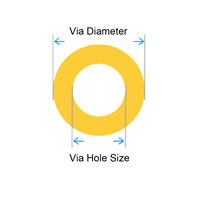
| Min. Via hole size/diameter | 0.15mm / 0.25mm |
1-layer (NPTH only): 0.3 mm hole size / 0.5 mm via diameter2-layer: 0.15mm hole size / 0.25mm via diameterMultilayer: 0.15 mm hole size / 0.25 mm via diameter ① Via diameter should be 0.1mm(0.15mm preferred) larger than Via hole size. ② Preferred Min. Via hole size: 0.2mm ③ 0.15mm hole size with any size via diameter, and 0.2mm / 0.25mm hole size with via diameter less than 0.45mm, will cost more. Please select corresponding via option when placing order. |
 |
| Min. Non-plated holes | 0.50mm | Please draw NPTHs in the mechanical layer or keep out layer. | 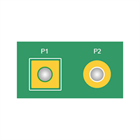 |
| Min. Plated Slots Width | 2-layer: 0.5mmMulti-layer: 0.35mm | The minimum plated slot width is 0.5mm, which is drawn with a pad.The length of the slot should be at least 2 times of the width. | 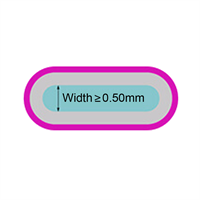 |
| Min. Non-Plated Slots | 1.0mm | The minimum Non-Plated Slot Width is 1.0mm, please draw the slot outline in the mechanical layer (GM1 or GKO) | 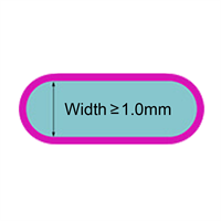 |
| Slot Hole size Tolerance | Plated: +0.13 / -0.08 mmNon-plated: ±0.2mm | Plated slot is made by drill tools.Non-plated slot is made by CNC. | |
| Via Hole-to-Hole Spacing | 0.2mm | Minimum center-to-center distance between two vias. | 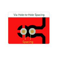 |
| Pad Hole-to-Hole Spacing | 0.45mm | Minimum center-to-center distance between two pads. | 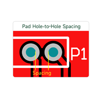 |
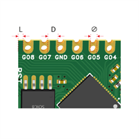
| Min. Castellated Holes | 0.5mm |
Castellated holes are metalized half-holes on PCB edges, commonly used on daughter boards to be soldered onto carrier PCBs. ① Hole diameter (Φ): ≥ 0.5 mm ② Hole to board edge (L): ≥ 1 mm ③ Hole to hole (D): ≥ 0.5 mm ④ Min. PCB size: 10 × 10 mm ⑤ Min. PCB thickness: ≥ 0.6 mm |
 |
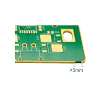
| Plated Edges | 10 × 10mm |
Plated edges are copper-plated and ENIG treated.HASL is not supported. ① Min. PCB size: 10 × 10 mm ② Min. PCB thickness: ≥ 0.6 mm ③ At least 3 breaks (more for larger PCBs) in the edge plating are required for support tab connections |
 |
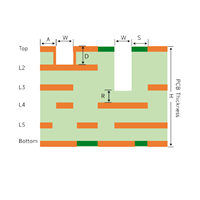
| Blind Slot | Supported |
① Blind slot width (W): ≥1.0mm ② Blind slot depth (D): ≥0.2mm ③ Blind slot annular width (A): ≥0.3mm (The pad width of PTH blind slots) ④ Safety distance (S): ≥0.2mm (The distance from NPTH blind slots to pad/traces/copper plane) ⑤ Blind slot remaining thickness (R): ≥0.2mm (The distance from the bottom of the blind slot to the nearest inner copper layer/surface substrate) ⑥ Supports 2-32-layer FR4 boards with a thickness of ≥0.8mm |
 |
| Backdrill | Supported |
Backdrill uses a secondary drilling process to control the depth of the hole, removing excess copper from the other layers of the via, thereby reducing its interference with the signal. ① Supports 4-32-layer FR4 boards with a thickness of ≥0.8mm ② Through-Hole Diameter(D): 0.2-0.5mm(Epoxy filled after backdrilling) ③ Backdrill Diameter(W): typically 0.2mm larger than through-hole diameter ④ Backdrill Depth(L): Layers with backdrilling, customizable ⑤ Dielectric Thickness(T): ≥0.15mm(from bottom of backdrill to the adjacent inner copper layer) ⑥ Safety Distance(S): ≥0.2mm(edge to pad/trace/copper safety distance) |
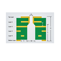 |
| Rectangular Holes / Slots | Not supported | Rectangular holes and slots without rounded corners are not supported. | 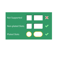 |
| Features | Capability | Description | Patterns |
| Min. track width and spacing (1 oz) | 0.10 / 0.10 mm (4 / 4 mil) | 1- and 2-layer: 0.10 / 0.10 mm (4 / 4 mil)Multilayer: 0.09 / 0.09 mm (3.5 / 3.5 mil). 3 mil is acceptable in BGA fan-outs. | 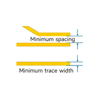 |
| Min. track width and spacing (2 oz) | 0.16 / 0.16 mm (6.5 / 6.5 mil) | 2-layer: 0.16 / 0.16 mm (6.5 / 6.5 mil)Multilayer: 0.15 / 0.15 mm (6 / 6 mil) | |
| Min. track width and spacing (2.5 oz) | 2 layer: 0.2/0.2mm(8mil/8mil) | — | |
| Min. track width and spacing (3.5 oz) | 2 layer: 0.25/0.25mm(10mil/10mil) | — | |
| Min. track width and spacing (4.5 oz) | 2 layer: 0.3/0.3mm(12mil/12mil) | — | |
| Track width tolerance | ±20% | e.g., For a 0.1 mm track, the finished track width ranges from 0.08 and 0.12 mm. | |
| PTH annular ring | ≥0.20mm | 2-layer:1 oz: Recommended 0.25 mm or above; absolute minimum 0.18 mm2 oz: 0.254 mm or aboveMultilayer:1 oz: Recommended 0.20 mm or above; absolute minimum 0.15 mm2 oz: 0.254 mm or above | 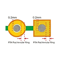 |
| NPTH pad annular ring | ≥0.45mm | Recommended 0.45 mm or more. This is to allow a 0.2 mm ring of copper to be removed around the hole for the sealing film to attach. Pad sizes smaller than the recommended value can result in the annular ring being very thin or completely missing. | 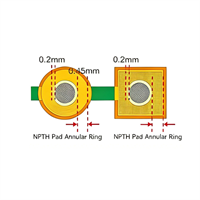 |
| BGA | 0.2mm | ① 0.2mm-0.25mm BGA pad diameter requires ENIG② BGA pad to trace clearance ≥ 0.1 mm (min. 0.09 mm for multilayer boards)③ Vias can be placed within BGA pads using filled and plated-over vias | 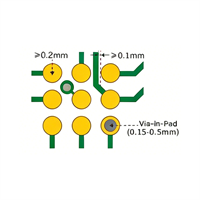 |
| Trace coils | 0.15/0.15mm | Minimum trace width/clearance: 0.15/0.15mm, when traces are covered by solder mask (1oz).Minimum trace width/clearance: 0.25/0.25mm, when traces are NOT covered by solder mask (1oz). ENIG only (high risk of short circuit with HASL) | 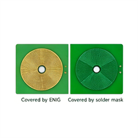 |
| Hatched grid width and spacing | 0.25 mm | Minimum width and spacing for hatched copper grids. | 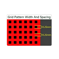 |
| Same-net track spacing | 0.25mm | Minimum spacing between two traces of the same net. | 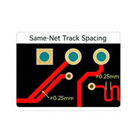 |
| Inner layer via hole to copper clearance | 0.2mm | Minimum clearance between via holes and copper on inner layers. | 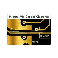 |
| Inner layer PTH pad hole to copper clearance | 0.3mm | Minimum clearance between PTH pads and copper on inner layers. | |
| Pad to track clearance | 0.1mm | Min. 0.1 mm (stay well above if possible). Min. 0.09 mm locally for BGA pads | 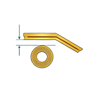 |
| SMD pad to pad clearance (different nets) | 0.15mm | More details of SMD pad spacing:SMD Components Minimum SpacingMinimum SMD pad: 0.25mm × 0.25mm | 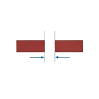 |
| Via hole to Track | 0.2mm | Minimum clearance between via holes and traces. | 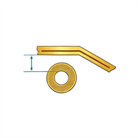 |
| PTH to Track | 0.28mm | 0.35mm is recommended, minimum 0.28mm | 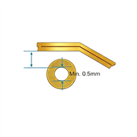 |
| NPTH to Track | 0.2mm | Minimum clearance between non-plated holes and traces. | 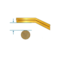 |
| Features | Capability | Description | Patterns |
| Soldermask Expansion | 1:01 | LDI equipment upgraded in June 2025. Pad size/soldermask opening will be 1:1 (Previous production file will be followed in Reorder).Keep at least 0.09 mm clearance between soldermask openings and neighboring traces. | 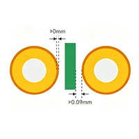 |
| Soldermask bridge | 0.10mm | 1oz copper:- Min. pad spacing: 0.10 mm (green, red, yellow, blue, purple)- Min. pad spacing: 0.13 mm (black, white)2oz copper:- Min. pad spacing: 0.20 mm (any color) | 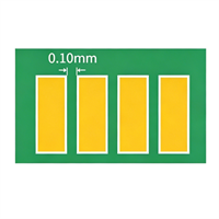 |
| Plugged vias | Filled with soldermask |
Vias are filled with soldermask for an opaque finish. ① Filled vias must not have soldermask openings on either side. ② Filled vias should have ≥ 0.35 mm clearance from other soldermask openings (e.g. pads). ③ Filled vias must be no wider than 0.5 mm diameter. |
 |
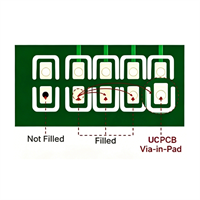
| UC PCB Via-in-Pad Process | Epoxy Filled & CappedCopper paste Filled & Capped |
Vias are filled with epoxy resin or copper paste and then plated over to achieve an opaque and smooth finish. ① Choose copper paste filling for applications requiring high thermal conductivity. ② This process is the default for 6-layer and above multilayer boards. ③ Compatible with via diameters from 0.15 to 0.55 mm. |
 |
| Solder mask dielectric constant | 3.8 | Typical dielectric constant of LPI (Liquid Photo Imageable) soldermask material. | 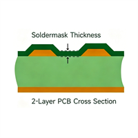 |
| Solder mask ink thickness | ≥ 10µm | Standard minimum thickness of the cured soldermask layer. |
| Features | Capability | Description | Patterns |
| Minimum Line Width | ≥0.15mm | Characters with line width less than 0.15mm will be unidentifiable. | 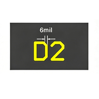 |
| Minimum text height | 40 mil (1.0mm) | Characters with height less than 40 mil (1.0mm) will be unidentifiable. | 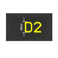 |
| Character width to height ratio | 1:06 | The preferred ratio of width to height is 1:6. | 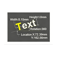 |
| Hollow-carved Character width to height ratio | 1:06 | The preferred ratio of width to height is 1:6. | 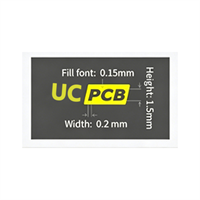 |
| Pad To Silkscreen | 0.15mm | The minimum distance between pad and silkscreen is 0.15mm. | 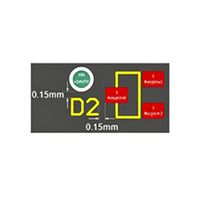 |
| Features | Capability | Description | Patterns |
| Routed | 0.2mm |
① Copper clearance from routed board edges: ≥ 0.2 mm ② Copper clearance from routed slots: ≥ 0.2 mm ③ Dimension tolerance for routed board edges: ±0.2 mm (regular precision); ±0.1 mm (high precision) ④ Minimum dimension 50×50mm for high precision, and at least 3 tooling holes with minimum 1.5mm diameter on different corners. ⑤ Minimum slot width for aluminum/copper core PCB: 1.6mm. |
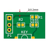 |
| V-Cut | 0.4mm |
① Copper clearance from V-cut board edges: ≥0.4 mm ② Dimension tolerance for V-cut board edges: ±0.4 mm. PCB thickness ≥ 0.6 mm ③ Zero panel board spacing by default. Alternatively, V-cut along one direction with no spacing and route along the other direction with 1.6 or 2 mm board spacing. ④ Min. panel dimensions: 70 × 70 mm; max. panel dimensions: 475 × 475 mm ⑤ V-cut groove angle: 25° ⑥ Minimum spacing between two v-cuts: 2mm (3mm is recommended) |
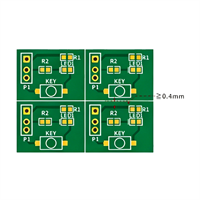 |
| Mouse bites Panel | 0.2mm |
① Copper clearance from non-mouse-bite board edges: ≥0.2 mm ② Dimension tolerance for non-mouse-bite board edges: ±0.2 mm (regular precision); ±0.1 mm (high precision) ③ Panel board spacing: 1.6 or 2 mm ④ Serrated edges will remain after depanelization ⑤ Minimum tooling edge width: 3 mm. For SMT assembly at JLCPCB, use 5 mm tooling edges, 2 mm tooling holes, and 1 mm fiducials centered at 3.85 mm from the panel edges. ⑥ Recommended diameter of mouse bite is 0.5mm-0.8mm; Recommended distance between the two mouse-bites is 0.2-0.3mm. The minimum width of breakaway tab is 4mm. For breakaway with mouse-bites, the minimum width is 5mm. |
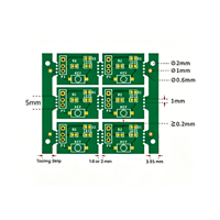 |
| Panelization with space | 2mm | The spacing between boards should be ≥ 2 mm, as narrow spacing results in difficulties for routing and V-cut. | 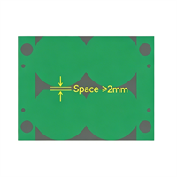 |
| Panel of Circular PCBs | ≥20mm×20mm | The single round board size should be ≥20mm×20mm when choose panel by JLCPCB. Panelize with stamp holes and add tooling strips on four board edges. | 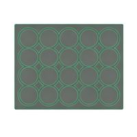 |
| Category | Features | Capability | Description |
| Layer Count | 1-layer,2-layers, 4-layers | The number of copper layers in the FPC | Rigid-flex PCBs are not yet supported. |
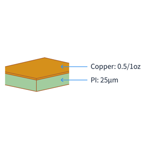
| FPC Stack-Up | 1-Layer (25µm dielectric thickness) |
FPC with copper and overlay on the same one side only. Inner PI thickness: 25 µm |
 |
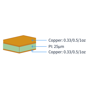
| 2-Layer (25µm dielectric thickness) |
FPC with copper on both sides. Inner PI thickness: 25 µm |
 |
|
| 1-layer (50µm dielectric thickness) | Tear-resistant. | 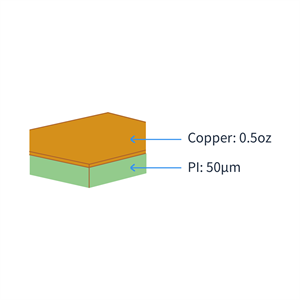 |
|
| 2-Layer (50µm dielectric thickness) | Tear-resistant. Suitable for impedance-controlled boards. | 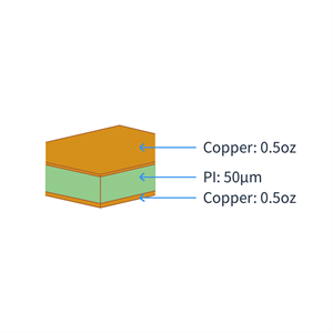 |
|
| 1-Layer (Transparent) | PET Thickness: 36um | 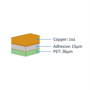 |
|
| 2-Layer (Transparent) | PET Thickness: 36um | 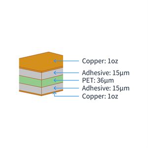 |
|
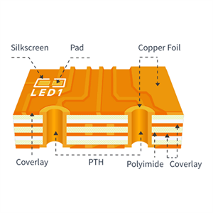
| 4-Layer |
Inner/outer layer copper weight: 1/3oz, 0.5oz, and 1oz. Lamination structures: with coverlay or without coverlay. For inner layers with 1oz copper weight, coverlay is applied by default to prevent delamination and blistering during lamination. |
 |
|
| Dimensions | Maximum Dimensions | Regular: 234 × 490 mm | Absolute limit of 250 × 600 mm allowed with edge rails – confirm with customer support before ordering. |
| Minimum Dimensions | No limit, but FPCs whose dimension is smaller than 20 × 20 mm are best panelised | See Flex PCB panel design guidelines | |
| FPC Finished Thickness |
25µm dielectric thickness FPC: 1-Layer: 0.07 / 0.11 mm 2-Layer: 0.11 / 0.12 / 0.2 mm 50µm dielectric thickness FPC: 1-Layer: 0.12 mm 2-Layer: 0.19 mm Transparent FPC: 1-Layer: 0.14 mm 2-Layer: 0.24 mm 4-Layer FPC: 0.2 / 0.25 / 0.30 / 0.35 / 0.40 / 0.45 mm |
①The thickness of the finished FPC excluding any stiffeners(If the measured area has no copper or coverlay, the finished thickness will be reduced.) ②White coverlay is 10um per side thicker than yellow/black coverlay. |
|
| Outer Layer Copper Weight |
Single-sided: 18 µm (0.5 oz), 35 µm (1 oz) Double-sided & four-layer: 12 µm (0.33 oz), 18 µm (0.5 oz), 35 µm (1 oz) |
The thickness of copper on the FPC | |
| Type of Process | Dry film process with LDI (laser direct image) exposure technology |
LDI provides higher accuracy than traditional LED exposure. The machines also support automatic alignment based on board size to eliminate pad offset issues. |
|
| Surface Finish | ENIG. Thickness: 1u” / 2u” | ENIG deposits a nickel-gold coating on exposed pads to prevent oxidation. | |
| Thickness with Stiffener | Thickness with Stiffener = FPC Thickness + Stiffener Thickness | See the PI Stiffener Thickness Calculator | |
| FPC Thickness Tolerance |
1. Area with stiffener thickness ≤ 0.3 mm: ±0.05 mm 2. Area with stiffener thickness between 0.3-1.0 mm(including 1.0 mm): ±0.1 mm 3. Area with stiffener thickness above 1.0 mm: ±10% 4. Gold finger area: ±0.03 mm |
Additional tolerance exists for stiffeners. Thicker stiffeners have larger tolerances. | |
| Holes | Hole Diameter | 0.1-6.5 mm | The recommended maximum diameter for PTHs is 5 mm, if bigger may cause risks to production |
| Diameter Tolerance | ±0.08 mm | Example: A 1.00 mm designed diameter is allowed to yield any physical diameter between 0.92-1.08 mm. | |
| Minimum Plated Slot | 0.50 mm | 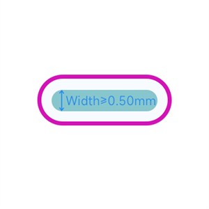 |
|
| Minimum Non-Plated Slot | Not limited | At least 0.2 mm copper clearance is required around non-plated slots. | |
| Castellated Holes |
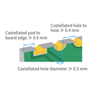
Castellated holes are plated half-holes on the edge of an FPC. Most often used for press-soldered connectors. ① Castellated hole diameter: ≥ 0.3 mm ② Castellated hole to board edge: ≥ 0.5 mm ③ Castellated hole to hole: ≥ 0.4 mm |
 |
|
| Min. Via hole size/diameter |
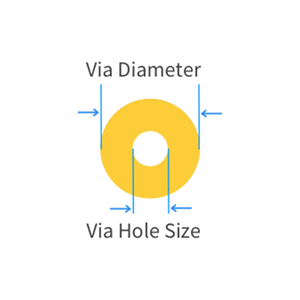
①Regular: 0.3mm/0.55mm ②Extreme for 2-layer: 0.10mm/0.3mm (extra cost required) ③Extreme for 4-layer: 0.15mm/0.35mm (extra cost required) ④Via diameter must be at least 0.2mm larger than via hole size, 0.25mm or above is better. |
 |
|
| Traces | Annular Ring for PTH | ≥ 0.25 mm recommended, absolute limit: 0.18 mm |  |
| Minimum Trace Width/Spacing (1 oz) |
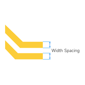
① 12 µm (0.33 oz) copper: 3/2 mil (absolute limit 2/2 mil – avoid if possible) ② 18 µm (0.5 oz) copper: 3.5/3.5 mil |
 |
|
| Trace Width Tolerance | ±20% | Example: A 0.10 mm designed trace width is allowed to yield any physical width between 0.08-0.12 mm. | |
| Pad-to-Trace Clearance |
① Via ring to trace: ≥ 0.1 mm (more whenever possible) ② Exposed pad to trace: ≥ 0.15 mm (more whenever possible) |
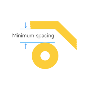 |
|
| NPTH to Copper Clearance | ≥ 0.20 mm | The clearance from an NPTH to traces, pads, and copper pours | |
| BGA |
① BGA pad diameter: ≥ 0.25 mm ② BGA pad to trace clearance: ≥ 0.2 mm |
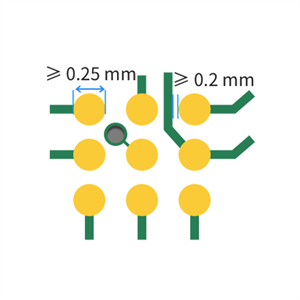 |
|
| Overlay/Soldermask | Coverlay Color | Yellow / Black / White / Transparent | Yellow is recommended |
| Coverlay Opening | Coverlay expansion (one-sided): 0.1 mm | 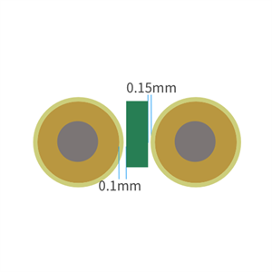 |
|
| Coverlay opening to trace clearance: ≥ 0.15 mm (more whenever possible) | |||
| Via covering | Recommended to keep coverlay over vias | ||
| Coverlay Thickness |
25µm dielectric thickness FPC: ① PI: 12.5µm, Adhesive: 15µm (on 1/3oz or 0.5oz copper) ② PI: 25µm, Adhesive: 25µm (on 1oz copper) 50µm dielectric thickness FPC: PI: 25µm, Adhesive: 25µm Transparent FPC: PET: 25µm, Adhesive: 25µm Note: white coverlay is usually 13-18µm thicker per side than yellow or black coverlay. |
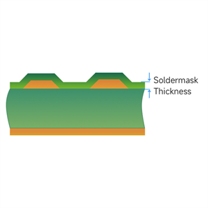 |
|
| Minimum solder bridge width |
0.5 mm minimum, i.e. solder bridge narrower than 0.5 mm will be removed. Contact customer support for any non-standard requirements. |
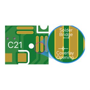 |
|
| Silkscreen | Character Height | ≥ 1mm (More in case of complex patterns or knock-out text) | 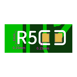 |
| Character Line Width | ≥ 0.15mm (Narrower lines do not print well) | ||
| Character to Pad Clearance | ≥ 0.15mm (Any silkscreen closer to a pad than this will be clipped) | ||
| FPC Outline | Laser Outline |
① Copper to board edge ≥ 0.3mm ② Copper to slots ≥ 0.3mm ③ Outline tolerance: ±0.1 mm (±0.05 mm upon request) |
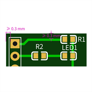 |
| Gold Finger Pad to Board Edge Clearance | 0.2 mm. Gold fingers will be cut back if exceeding this clearance to avoid damage during laser cutting the outline. Castellated pads are exempt from this clearance. | 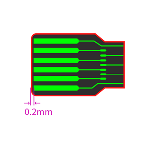 |
|
| Panels (See FPC Panel Design Guide) |
① Spacing between boards is commonly 2 mm. For boards with metal stiffeners use 3 mm instead. ② Handling edges of width 5 mm required on all four sides. Copper is required on these edges, with 1 mm clearance around fiducials and 0.5 mm clearance around tooling holes. ③ Fiducials: 1 mm; tooling holes: 2 mm; Fiducial centre to board edge: 3.85 mm. Add four fiducials with one offset by 5 mm or more to aid orientation. ④ Support tab width: 0.7-1.0 mm ⑤ Maximum panel size: 234 × 490 mm |
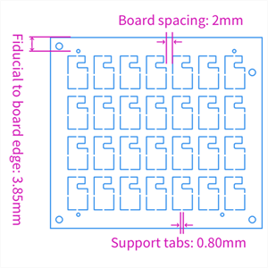 |
|
| Stiffeners (Detailed Introduction) | PI Stiffener | Thickness options: 0.1 mm, 0.15 mm, 0.20 mm, 0.225 mm, 0.25 mm | PI stiffeners are most often used with gold finger connectors. For example if the connector needs to be 0.3 mm thick on a 0.11 mm FPC, a 0.225 mm stiffener thickness is most suitable. |
| FR4 Stiffener | Thickness options: 0.1 mm, 0.2 mm, 0.4mm, 0.6mm, 0.8mm, 1.0mm, 1.2mm, 1.6mm (bonding with adhesive under high temperature and pressure) | FR4 is usually only used on low-end products because it is prone to chipping. Avoid if possible. | |
| Stainless Steel Stiffener | Thickness options: 0.1 mm, 0.2 mm, 0.3 mm | Steel stiffeners cost more but have excellent flatness and do not easily deform. This makes them good as support under SMD components. Note that since steel is slightly magnetic it should not be used with hall effect sensors or similar components. | |
| 3M Tape | 3M9077 (0.05 mm thick; heat-resistant)3M468 (0.13 mm thick; not heat-resistant)tesa8854 (0.1mm thick; heat-resistant, good adhesion, recommended) | Usually used to secure FPCs after assembly | |
| EM Shielding Film | 18 µm thick, black. Helps lower EMC. The recommended practice is to add soldermask openings to electrically connect ground plane with the shield films. | 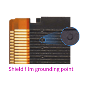 |
|
| Design Considerations | Impedance Calculation | Core polyimide cr. 3.3 | Impedance measurement and control are not yet supported. Traces are only controlled for width and the customer is responsible for choosing trace widths to achieve their impedance requirements. UCPCB provides impedance reference line widths; see details. |
| Coverlay cr: 2.9 | |||
| Core polyimide thickness: 25 µm / 50 µm | |||
| EasyEDA (Highly Recommended) | EasyEDA supports a dedicated stiffener layer. The shape and thickness of stiffeners are set and embedded in the design document so they don’t need to be entered manually when ordering. | 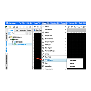 |
|
| See how to design FPC at EasyEDA | |||
| Other EDA Software | Indicate materials on silk screen layer. This information is not in the stiffeners part so the fabrication does not know. Check the order before ordering. Make sure that annotation texts do not overlap the board area. | 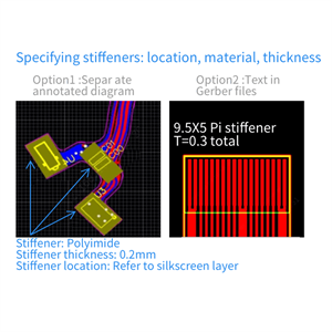 |
|
| Other Design Constraints | Same requirements as rigid PCBs in terms of holes, traces, soldermask, and silkscreen. |
| Features | Economic PCBA | Standard PCBA |
| Assembly Types | Single sided placement (SMT/Thru-hole) | Single & double sided placement (SMT/Thru-hole) |
| PCB Layer | 2,4,6-layers | 1 - 32 layers |
| Thickness | 0.8mm - 1.6mm | No limit |
| Dimension | Single PCB Size: 10×10mm - 470×500mm | Single PCB Size: 70×70mm - 460×500mm |
| PCB Panel Size: 10×10mm - 250×250mm | PCB Panel Size: 70×70mm - 250×250mm | |
| Order Volume | 2 - 50 pcs | 2 - 80000 pcs |
| Surface Finish | Limited by specific options (Refer to the options for Economic PCBA in the table below) | No limit |
| PCB Color | Limited by specific options (Refer to the options for Economic PCBA in the table below) | No limit |
| Delivery Format | Single PCB, Panel with mouse bites | Single PCB, Panel with mouse bites, Panel with V-cut |
| Layer Stackup | Standard stack-up only, special stack-up is not supported | All stack-up |
| Gold Fingers/Castellated Holes/Edge Plating | Not Support | Support |
| Edge Rails | Not necessary | Necessary |
| Fiducials | Not necessary | Necessary |
| Minimum Package | 402 | 201 |
| Minimum IC Pin Spacing | 0.4mm | 0.35mm |
| Minimum BGA Spacing | 0.5mm(center to center) | 0.35mm(center to center) |
| Reflow temperature | 255+/-5 ℃ (not adjustable) | 240+/-5 ℃ |
| SPI | No | Yes |
| AOI | Yes | Yes |
| Visual Inspection | Yes | Yes |
| X-ray Inspection | Yes (only for certain parts, such as BGA) | Yes (only for certain parts, such as BGA) |
| Build time | 1 - 3 days | ≥ 4 days |
| Layer | Thickness(mm) | Color | Surface Finish | Qty(pcs) |
| 2L | 0.8 | Green | Lead-Free:HASL、Leaded:HASL | 2-30 |
| 1 | Green/Black | Lead-Free:HASL、Leaded:HASL | 2-30 | |
| 1.2 | Green/Black | Lead-Free:HASL、Leaded:HASL | 2-30 | |
| 1.6 | Green | Lead-Free:HASL / ENIG、Leaded:HASL / ENIG | 2-50 | |
| 1.6 | Black | Lead-Free:HASL、Leaded:HASL | 2-50 | |
| 1.6 | Blue/Purple | Lead-Free:HASL、Leaded:HASL | 5—30 | |
| 1.6 | Red/White | Leaded:HASL | 5—30 | |
| 4L | 1 | Green | Lead-Free:HASL、Leaded:HASL | 2-30 |
| 1.2 | Green | Lead-Free:HASL、Leaded:HASL | 2-50 | |
| 1.6 | Green | Lead-Free:HASL / ENIG、Leaded:HASL / ENIG | 2-50 | |
| 6L | 1.6 | Green | ENIG | 2-30 |
| Feature | Capabilities |
| Stencil Types | Framework & Non-Framework |
| Stencil Material | 304 HTA stainless steel |
| Minimum Aperture Size | >0.08mm |
| Cutting Tolerance | ±0.003mm |
| Cutting Technology | Precision Laser Cutting |
| Manufacturing Capabilities | Over 30 laser cutting machines in operation |
| Stencil File Formats | Gerber files (with solder paste layers), DXF |
| Thickness |
Select by UCPCB Our engineers will select an appropriate thickness based on your design from the standard thickness. Select by customer If you wish to specify the thickness by yourself, please select 'Select by Customer'. Standard thickness ( no extra cost): 0.10 mm, 0.12 mm, 0.15 mm, 0.18 mm, 0.20 mm. Special thickness (with extra cost): 0.03mm, 0.04mm, 0.05mm,0.06mm,0.08mm,0.25mm,0.3mm,0.4mm,0.5mm. |
| Dimensions |
Non-Framework:Standard size: 280×380mm- 700 × 600 mmCustom size: You can customize any dimensions within 650580mm.Note: Any non-standard sizes, for example, 1:1 as PCB, need to choose custom size and input specific size. Framework:Minimum: 400×300(Valid Area:240mm140mm)Square Max: 736 × 736 mm (Valid Area: 500 × 500 mm)Rectangular Max: 1500 × 500 mm (Valid Area: 1300 × 320 mm) Note:Valid Area is where the apertures can be open |
| Nano-Coating | Available for all types of stencils |
| Step Stencil | Only available for stencils with framework |
| Ultrasonic-Resistant Adhesive | Only available for stencils with framework |
| Stencil Side |
4 options: 1.Top Only 2.Bottom Only 3.Top + Bottom (On Single Stencil) 4.Top + Bottom (On Separate Stencils)Learn more on the quote page. |
| Stencil Process Type |
2 options: 1.Solder Paste Stencil 2.Red Glue Stencil Learn more on the quote page. |
| Polishing Process |
3 options: 1.Sanding 2.Etching Polish 3.Electropolishing (Ideal for ICs ≤ 0.5 mm pitch and BGA packages) Learn more on the quote page. |
| Fiducials |
3 options: 1.No Fiducial 2.Etched Through 3.Etched Half IntoLearn more on the quote page. |
| Stencil Package |
Non-framework: ≤250×250 mm: Packed in a plastic bag with an air-shipping box.>250×250 mm: Packed in a cardboard box and clamped with wooden boards. Framework: Packed in a box, then clamped with wooden boards |
| Build Time |
Fastest build time: 12 hours Note: The final build time may vary based on the selected stencil specifications and order confirmation time. |
| Stencil Delivery |
If you order a stencil together with PCBs, stencil size within 280mm × 280mm can be shipped together with the PCBs. However, if you choose express shipping (e.g., DHL, FedEx), stencil size exceeding 280mm × 280mm will be shipped separately. |
Professional PCBA manufacturer in China, providing one-stop manufacturing services with excellent quality and service.
Room 602 & 603, Building C, Qianwan Key & Core Technology Industrial Park, Bao'an District, Shenzhen, China
Copyright © Shenzhen UC Industrial Limited All Rights Reserved Privacy Policy
 EN
EN