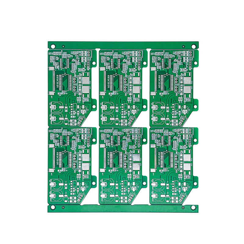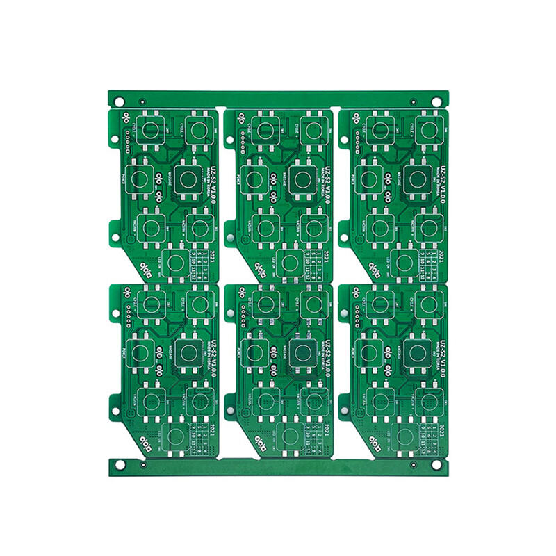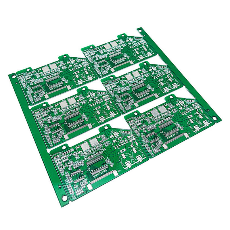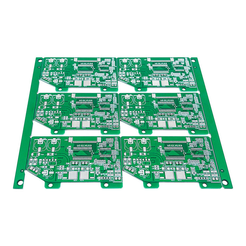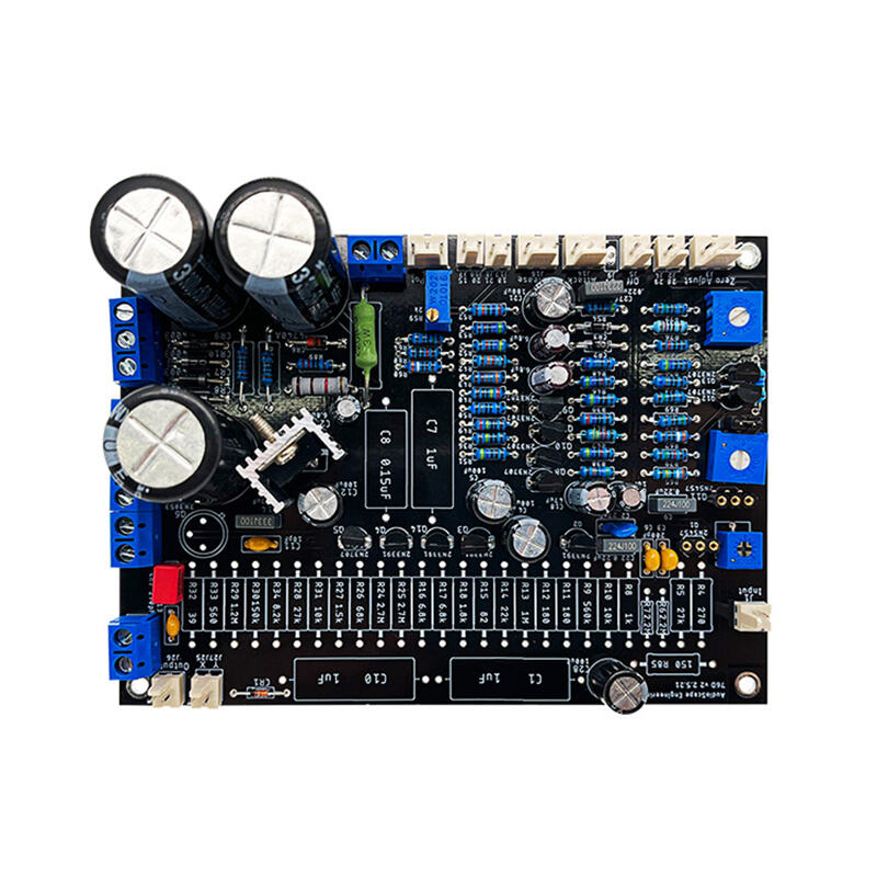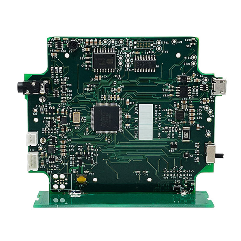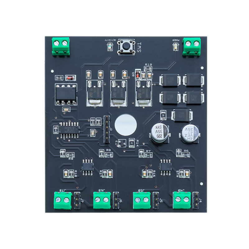
This high-precision 2×3 panelized multilayer PCB board is engineered for smart electronic devices, featuring a green solder mask and advanced circuit design to support compact component integration. The panelized structure optimizes production efficiency, reducing handling costs and improving yield during mass manufacturing.
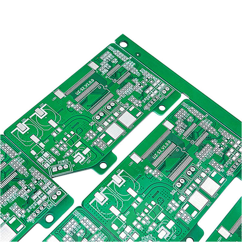
With precise trace routing and reliable component pads, this PCB ensures stable signal transmission and excellent thermal management for smart home, consumer electronics, and industrial IoT applications. Manufactured in compliance with IPC standards, it offers superior electrical performance and durability, making it an ideal choice for high-volume electronic product development.
| Place of Origin | China (Mainland) |
| Brand Name | Customizable (OEM/ODM supported) |
| Model Number | PAN-PCB-006 (customizable) |
| Certification | ISO9001, RoHS, IPC Class 2/3, UL |
| Base Material | FR-4 Tg130/Tg150 (customizable) |
| Layers | 4-6 layers (customizable) |
| Surface Finish | Immersion Silver / ENIG / HASL |
| Solder Mask | Green (other colors available) |
| Board Thickness | 1.2mm / 1.6mm (customizable) |
| Copper Thickness | 1oz / 2oz (customizable) |
| Panel Size | Customizable (2×3 array as shown) |
| Minimum Trace Width | 0.1mm (customizable) |
| Minimum Hole Size | 0.2mm (customizable) |
· Smart home devices & IoT sensors
· Consumer electronics (wearables, smart controllers)
· Industrial automation & monitoring modules
· Automotive electronics (infotainment, control systems)
1. Efficient Panelization: 2×3 array design maximizes production yield and reduces assembly costs.
2. High Precision: Advanced lithography and etching ensure accurate trace alignment for high-frequency signals.
3. Reliable Performance: RoHS-compliant materials and strict quality control guarantee long-term stability.
4. Customizable Design: Flexible layer count, thickness, and surface finish to meet diverse project needs.
5. Thermal Management: Optimized copper distribution supports effective heat dissipation for power components.
Q: What is the advantage of panelized PCB design?
A: Panelization reduces handling time, minimizes material waste, and improves production efficiency, making it ideal for high-volume manufacturing.
Q: Can I customize the panel size and number of units per panel?
A: Yes, we support fully customized panel layouts (e.g., 2×2, 3×5) to match your production line and assembly requirements.
Q: What surface finish options are available for this PCB?
A: We offer ENIG (Electroless Nickel Immersion Gold), immersion silver, and HASL (Hot Air Solder Leveling) to suit different soldering and reliability needs.
Professional PCBA manufacturer in China, providing one-stop manufacturing services with excellent quality and service.
Room 602 & 603, Building C, Qianwan Key & Core Technology Industrial Park, Bao'an District, Shenzhen, China
Copyright © Shenzhen UC Industrial Limited All Rights Reserved Privacy Policy