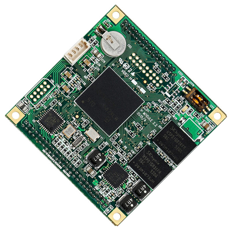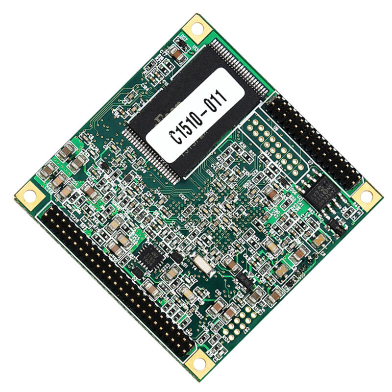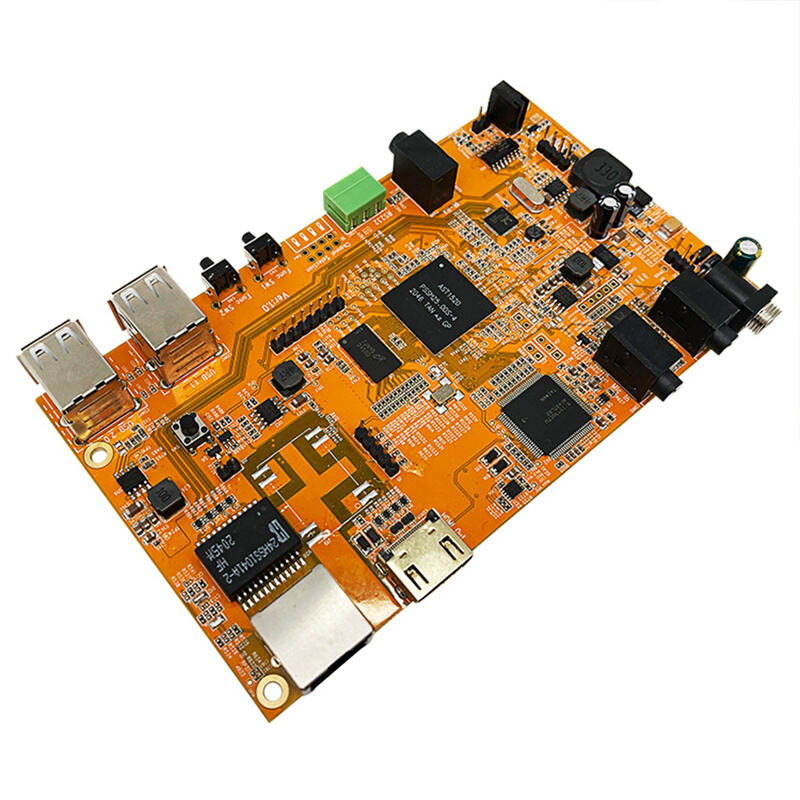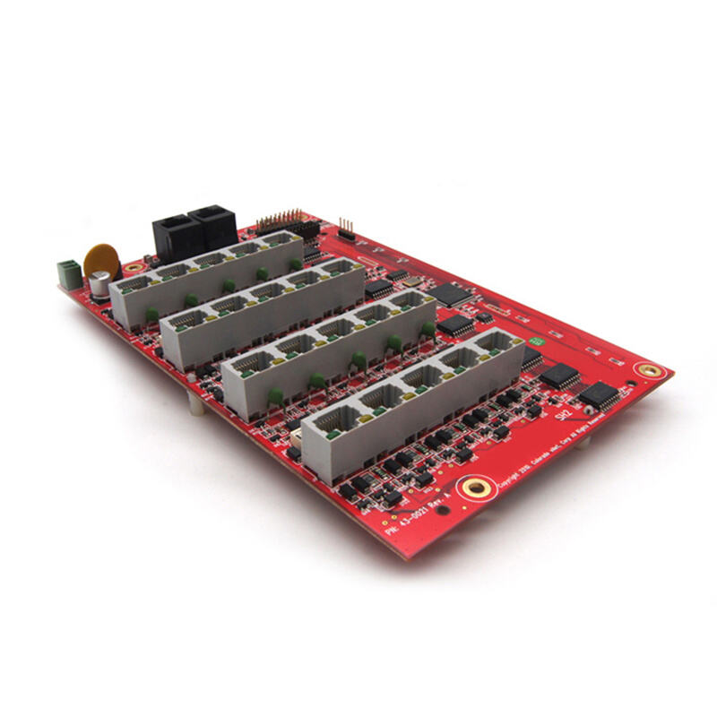
This high-density system-on-module (SOM) core board is engineered for advanced industrial embedded applications, integrating a powerful FPGA (Field-Programmable Gate Array) as the main processing unit. Built on a premium FR-4 substrate with precise multi-layer routing, it combines high-speed signal processing, large-capacity data storage, and reliable power management in a compact form factor.
The board features Hynix semiconductor memory chips for high-speed data access and storage, a coin-cell battery holder for real-time clock (RTC) backup, and extensive pin header interfaces for seamless system expansion. Designed for flexibility and performance, it supports custom logic implementation via the FPGA, making it ideal for high-speed image processing, industrial control, communication gateways, and intelligent instrumentation systems.
Compliant with IPC Class 2/3 and RoHS standards, the module undergoes rigorous environmental and quality testing to ensure stable operation in harsh industrial conditions. Whether for complex algorithm acceleration or versatile I/O expansion, this FPGA core board provides a powerful, scalable solution for cutting-edge embedded development and mass production.
| Place of Origin | China (Mainland) |
| Brand Name | Customizable (OEM/ODM supported) |
| Model Number | SOM-FPGA-CORE-001 (customizable) |
| Certification | ISO9001, RoHS, CE |
| Base Material | FR-4 Glass Epoxy (High Tg optional) |
| Layers | 6-8 layers (high-speed design) |
| Board Thickness | 1.6mm |
| Surface Finish | ENIG / HASL (Lead-free) |
| Solder Mask | Green |
| Core Processor | High-performance FPGA (customizable model) |
| Memory | Hynix DDR3/DDR4 SDRAM + Flash (capacity customizable) |
| Peripherals | RTC Battery Holder, Pin Headers, Expansion Ports, JTAG Interface |
| Power Input | 5V DC (or customizable voltage) |
| Operating Temperature | -40°C ~ +85°C (Industrial Grade) |
| Assembly Type | High-precision SMT assembly |
· Industrial automation & motion control systems
· High-speed image processing & machine vision
· Intelligent communication gateways & network switches
· Medical imaging & diagnostic equipment
· Aerospace & military embedded computing modules
1. Powerful FPGA Architecture: Dedicated FPGA chip supports parallel processing and custom logic design, ideal for high-computation tasks.
2. High-Speed Memory: Integrated Hynix memory ensures fast data access and large-capacity storage for complex applications.
3. Comprehensive Connectivity: Abundant pin headers and expansion ports simplify connection to sensors, actuators, and external systems.
4. RTC Backup: Onboard battery holder ensures reliable system timekeeping during power outages.
5. Compact & Reliable: Space-saving SOM design reduces system size while maintaining industrial-grade stability and durability.
Q: Can the FPGA chip model and memory capacity be customized?
A: Yes, we offer full customization of core chip selection, memory capacity, and I/O configuration to meet specific performance requirements.
Q: Does this module support software development and FPGA programming?
A: Yes, we provide technical support for FPGA firmware development, driver integration, and system software customization.
Q: What is the typical lead time for mass production?
A: Mass production lead time is approximately 20-25 days; sample development and delivery are available within 10-15 days.
Professional PCBA manufacturer in China, providing one-stop manufacturing services with excellent quality and service.
Room 602 & 603, Building C, Qianwan Key & Core Technology Industrial Park, Bao'an District, Shenzhen, China
Copyright © Shenzhen UC Industrial Limited All Rights Reserved Privacy Policy