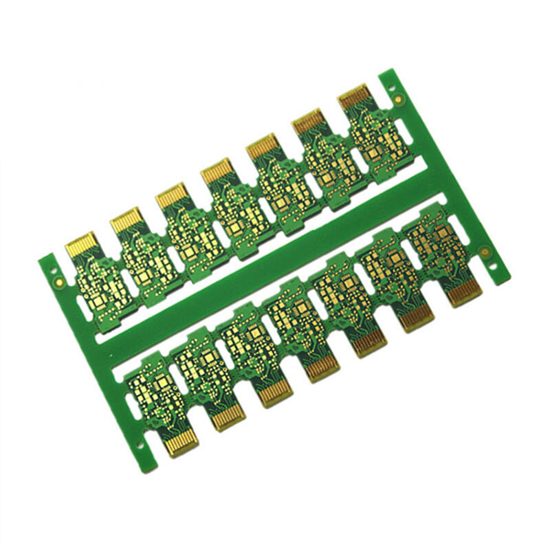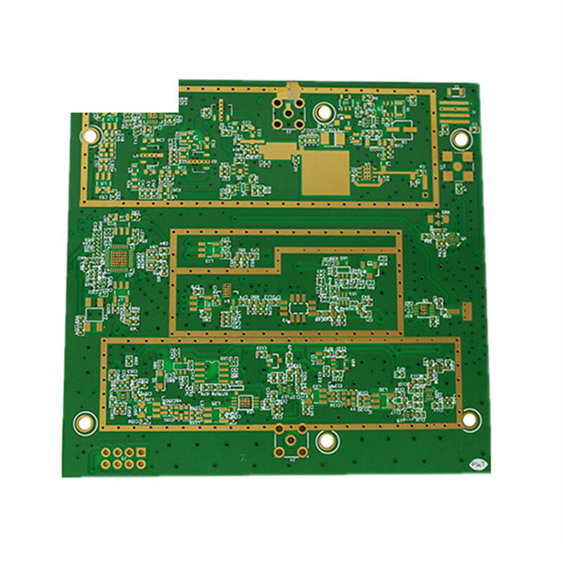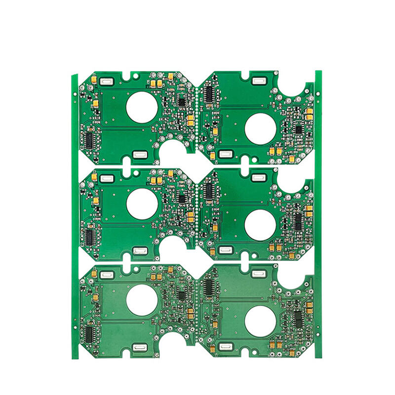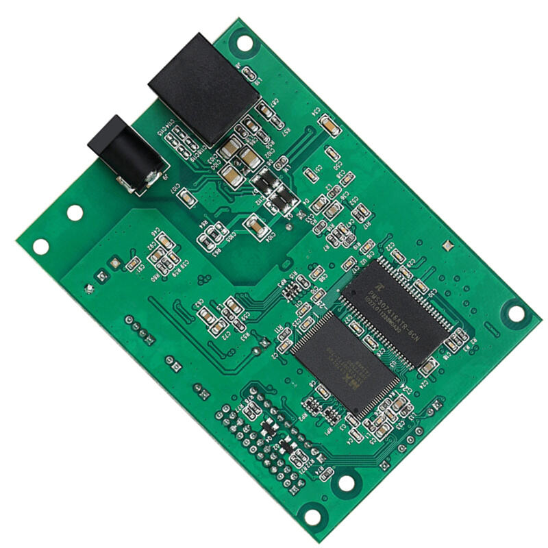
This multi-panel rigid PCB is specially designed for USB flash drive and portable storage device applications, featuring a high-efficiency array layout that supports mass production and automated assembly. Constructed from high-quality FR-4 substrate, it delivers excellent mechanical stability, thermal resistance, and electrical reliability, ensuring consistent performance in compact storage devices.
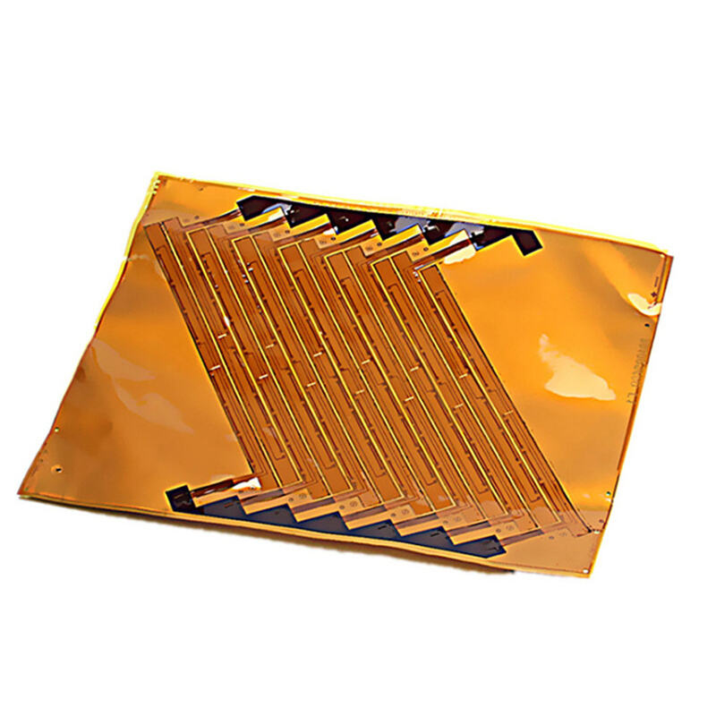
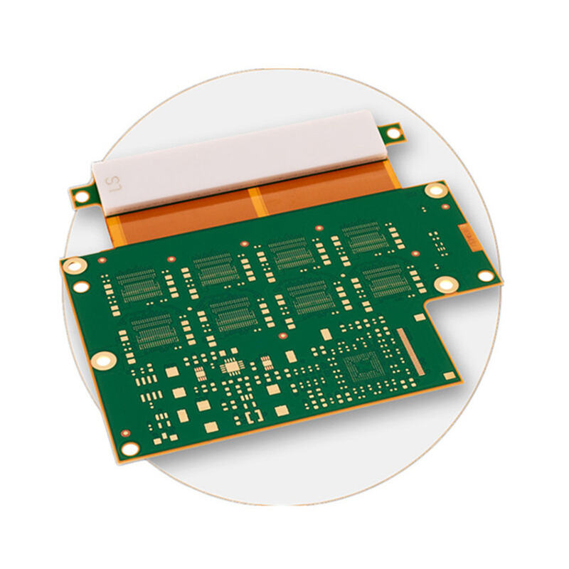
Equipped with precision-etched circuits and gold-plated edge connectors, this PCB provides reliable signal transmission and durable plug-and-play functionality, critical for USB interface applications. The multi-panel array design (with multiple individual PCBs integrated into a single panel) streamlines SMT assembly, testing, and depaneling processes, significantly improving production efficiency and reducing manufacturing costs. The fine-pitch component pads are optimized for small SMD components, enabling high-density integration in ultra-compact form factors.
Our advanced manufacturing process ensures tight impedance control, low signal loss, and uniform surface finish, meeting the strict quality requirements of consumer electronics. We offer full customization services, including panel layout, connector pin count, and component pad design, to match your specific product specifications. Whether for USB 3.0/3.1/3.2 flash drives, portable SSDs, or other storage peripherals, this multi-panel rigid PCB provides a cost-effective, high-performance foundation that accelerates product development and scales with mass production.
| Place of Origin | China |
| Brand Name | [Your Brand] |
| Model Number | USB-Storage-MultiPanel-PCB-007 |
| Certification | RoHS, REACH, ISO 9001, IPC-6012 |
| Base Material | FR-4 (TG130) |
| Conductor Material | Electrodeposited Copper (1oz) |
| Layer Count | 2–4 layers (customizable) |
| Minimum Line Width | 0.075mm |
| Minimum Line Spacing | 0.075mm |
| Board Thickness | 0.4mm–0.8mm (customizable) |
| Surface Finish | ENIG (gold-plated edge connector) + OSP |
| Panel Layout | Multi-unit array (customizable count) |
| Connector Type | Gold-plated USB edge connector (Type-A/Type-C optional) |
| Operating Temperature | -20°C to +85°C |
| Depaneling Method | V-cut / punching (customizable) |
· USB Flash Drives: Used in USB 2.0/3.0/3.1/3.2 flash drives for high-speed data storage and transfer.
· Portable Storage: Integrated into portable SSDs and mini storage devices for compact, reliable performance.
· Consumer Electronics: Applied in card readers, USB adapters, and other compact peripheral devices.
· Mass Production: Ideal for high-volume consumer electronics manufacturing, supporting automated SMT and testing lines.
1. Multi-Panel Efficiency: Array panel design maximizes material utilization and streamlines automated production.
2. Gold-Plated Connectors: Durable gold-plated edge connectors ensure reliable USB signal transmission and long plug life.
3. High-Density Integration: Fine-pitch pads enable compact component placement for ultra-small storage devices.
4. Cost-Effective Manufacturing: Optimized panel layout reduces assembly time and per-unit production costs.
5. Full Customization: Tailored to panel count, connector type, and component layout to match your product design.
Q: Can I customize the number of units per panel for this USB PCB?
A: Yes, we can adjust the panel layout to include any number of individual USB PCBs, based on your production line requirements.
Q: What USB connector types are supported?
A: We support gold-plated edge connectors for Type-A, Type-C, and other standard USB interfaces, customizable to your product design.
Q: What is the lead time for this multi-panel PCB sample and mass production?
A: Sample lead time is typically 3–5 working days, while mass production lead time is 5–10 working days, depending on order quantity and panel complexity.
Q: Is this PCB compatible with high-speed USB 3.2/4.0 protocols?
A: Yes, our precision impedance control and low-loss materials support high-speed USB 3.2/4.0 signal transmission requirements.
Professional PCBA manufacturer in China, providing one-stop manufacturing services with excellent quality and service.
Room 602 & 603, Building C, Qianwan Key & Core Technology Industrial Park, Bao'an District, Shenzhen, China
Copyright © Shenzhen UC Industrial Limited All Rights Reserved Privacy Policy